Automatic Litter Box -Hand-Soldered PCB — Wiring the System Together
At this stage of the project, things started to get messy.
Multiple modules, loose wires, temporary connections… it worked — but it wasn’t sustainable.
So instead of spending a lot of time designing a perfect PCB in KiCad, I took a more practical approach:
👉 I built my own PCB by hand.
🧠 Why Not KiCad (Yet)?
I initially started designing a proper PCB in KiCad.
But:
- The learning curve is steep
- Layout + routing takes time
- Multiple iterations are needed
For this phase of the project, that didn’t make sense.
I needed something working now, not perfect later.
So I switched approach.
🔧 The Solution — Perfboard PCB
I used a standard prototyping board and soldered everything manually.
📸 The Board
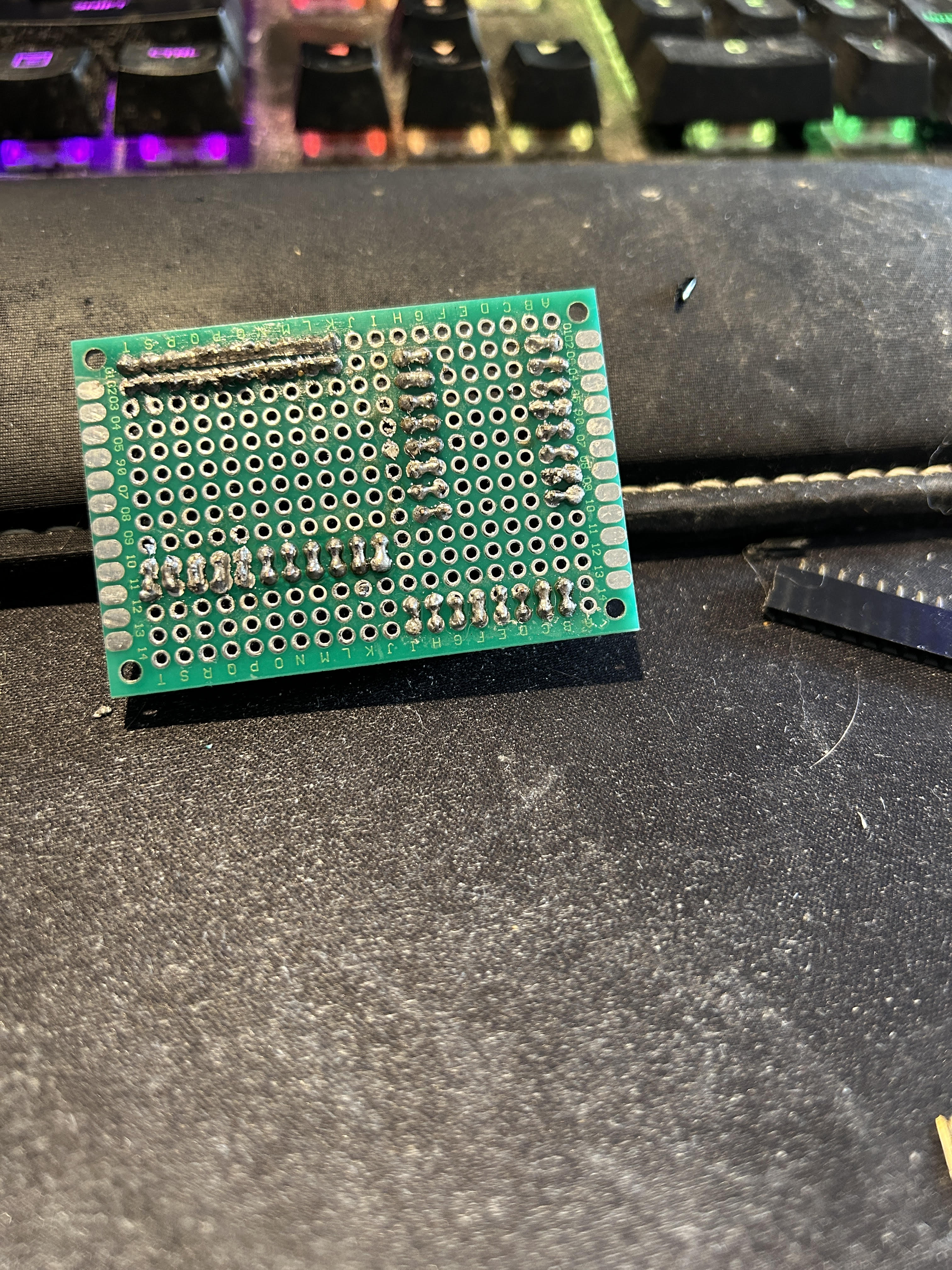
🎯 Purpose of This Board
This PCB acts as a central wiring hub.
Instead of:
- Loose jumper wires
- Unstable breadboard connections
- Debugging random disconnects
Everything is now:
- done led test to see if things are dual connected so I dont get short circuit.
- Fixed
- Repeatable
- Easier to troubleshoot
🔌 Components Connected (Current Plan)
This board will handle connections for:
- HX711 Module (load cell for weight detection)
- 1.3" OLED (128x64, I2C)
- TB6600 stepper driver
- NEMA 23 motor
- KY-023 Joystick module
And likely more components later.
⚙️ What This Improves
1. Stability
No more loose wires = fewer random issues.
2. Debugging
You can now:
- Trace connections visually
- Probe signals easily
- Isolate problems faster
3. Expandability
Even though it's handmade, it’s structured enough to:
- Add new modules
- Reroute signals if needed
⚠️ Tradeoffs
This isn’t a “clean” PCB:
- No ground plane
- No optimized routing
- Not production-ready
But that’s fine.
This is a functional prototype board.
🧠 Key Insight
Sometimes the fastest way forward isn’t the “correct” way.
It’s the way that:
- Gets you unstuck
- Lets you test ideas
- Keeps momentum going
This board does exactly that.
🔜 Next Step
Once the system is stable and finalized:
👉 Then it makes sense to design a proper PCB in KiCad.
At that point:
- Requirements are clear
- Layout is known
- Fewer iterations needed
🧪 Summary
- Skipped full PCB design (for now)
- Built a hand-soldered wiring hub
- Connected all major modules
- System is now more stable and maintainable
This is one of those “ugly but important” steps that makes everything else possible.
Comments
Comments
Loading comments…